NANO PATCH-CLAMP (NPC)
DEVELOPMENT OF A HIGH-THROUGHPUT SYSTEM BASED ON PLANAR PATCH-CLAMP
"Patch clamping is a marvelous technique. It allows you to have access to currents across a cell in two ways: one is to look at very few channels, very few molecules, or to look at the whole cell with high resolution." Francisco Bezanilla of the University of California.
The Patch Clamp is nawdays the electrophysiological technique of election
to investigate ion channels. Ion channels are transmembrane proteins
involved in nearly all physiological processes and in many human diseases,
still today a membrane protein class in continuous exploration. The
scientific interest for these proteins is manifested by base search,
to the aim to comprise its structure, function and pharmacology, and
by applied search biomedical and farmaceutical, for the screening
of new drugs.
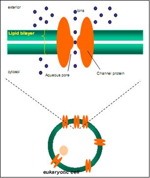
Figure
1. Schematic view of an eukaryotic cell and its ion channels.
Even if
traditional patch-clamp method has transformed both neuroscience and biophysics
helping usher in a new branch of drug-development research focused on
ion channels, these proteins remain an under-exploited target class, which
is in large part due to the labour-intensive and low-throughput nature
of the technique of election. However, traditional patch approache work
well in academia, where only researchers perform individual experiments.
Industry, where streamlining and throughput are important, as well as
functional genomics projects or screenings for neuroscience and pharmaceutical
research, require assays with a much higher throughput.
Several companies have released or are planning to release commercial
implementations of a new high-throughput variation on the technique, called
planar patch clamping. In these automatic devices like the planar population
array patch-clamp, PAPC, the micropipettes are replaced by pores in planar
supports. Our primary intention was to achieve a high-throughput system
based on PAPC. We rely on a Nano Patch-Clamp (NPC) device based on poly(dimethylsiloxane)
(PDMS) planar chips because of high processability and low cost of that
alternative material used instead of glass, quartz or silicon.
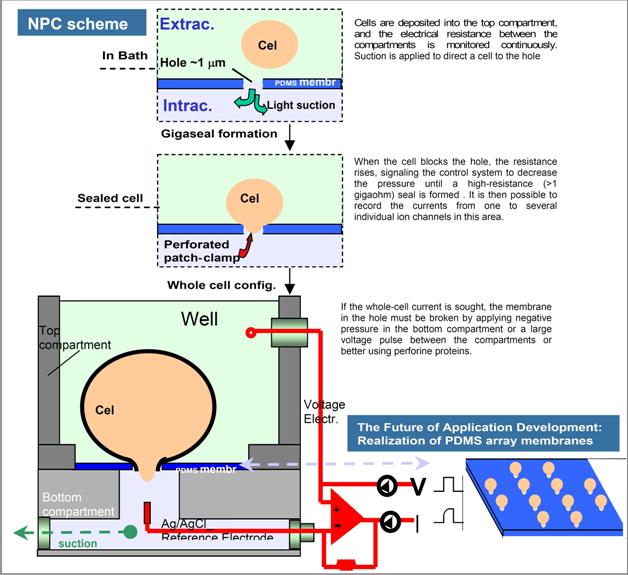
Figure 2. Schematic drawing. Establishing the whole-cell recording configuration with the prototype planar Patch-Clamp chamber. The whole procedure of preparing the whole-cell configuration is summarized into 3 states: in bath, sealed cell and whole-cell
Our microfabrication
and processing technology is sufficiently mature to produce a consistent
single-channel prototype of NPC system. Planar polymeric chips, obtained
combinig soft-lithography and air-molding, and altered to be hydrophilic
by rapid oxygen plasma treatment, have been developed. PDMS Chips will
be used in a plexiglass bench-top device. Scanning Electron Microscopy
(SEM) and precise Focused Ion Beam (FIB) systems are used to determine
the characteristics of the PDMS cell-pore interface. Our device has been
validated using both suspended and adherent cells. We are able to obtein
gigaselas and we are currently in the process of realizing whole-cell
configuration by using perforine proteins. The nearly future of application
development is the realization of a relatively low-cost PDMS array support
to perform simultaneous parallel automated recordings.
MAKING THE PDMS PLANAR CHIPS
Fabrication
of Silicon Masters
The FIB system uses a Ga+ ion beam to raster over the surface of a silicon
master. The ion beam allows the milling of small holes in the sample at
well localized sites _Fig. 3.
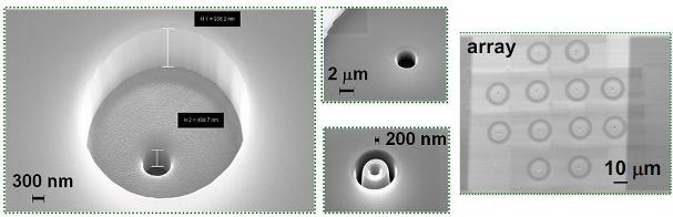
Figure
3.SEM
images. Creation of different micropore conformations with FIB, after
the Si-master is fixed on a pyrex support.
Soft
Lithography
Soft lithography is a process which allows a pattern on a master to be
embossed on soft substrate: polydimethylsiloxane, PDMS. The stamp on the
master defines the shape of the final PDMS structure. The soft lithography
is especially powerful because it is inexpensive and quick to make many
structures from the same master _ Fig. 4.
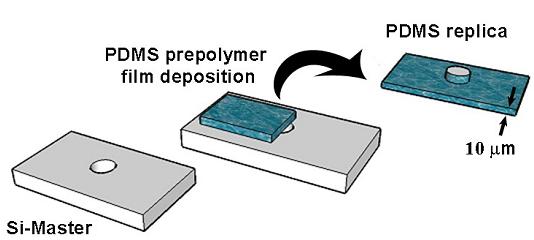
Figure
4.
Using Soft-Lithography the master is covered with PDMS prepolymer and
spinned to have 10 um thick film. After curation the PDMS replica is peeled
off from the Si-master coating it to a perfrated PDMS disch.
Air
Molding
An experimental set-up for implementing the air molding technique in a
highly flexible way has been designed, developed and tested. This apparatus
uses a nitrogen stream, channeled through the micro-perforated silicon
master, to shape a smooth micrometric pore in the PDMS thin film _ Fig.
5.
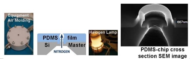
Figure
5. A: The PDMS film is perforated by air-molding then cured using
an halogen lamp.
Oxygen
Plasma
This surface treatment removes organic residues and chemically reacts
with the surface to form strong covalent carbon-oxygen bonds, which are
much more polar and more reactive than the initial carbon-hydrogen bonds.
Before making an experiment the PDMS replica is exposed to oxygen plasma
surface treatment, to change its surface from hydrophobic to hydrophilic.
Experimental
Patch-Clamp prototype chamber
A PDMS replica is positioned between top and bottom compartments of the
chamber _Fig. 6. 10 ml of lymphocytes CEM cell suspension in extracellular
working solution (±104 cells) is added to the external well. Experiments
start when cells are attached to the PDMS-chip surface, within 5'-10'.
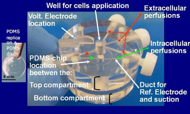
Figure6.
Patch-Clamp prototype chamber and PDMS replica fixed on PDMS disch.
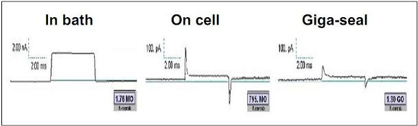
Experimental
Results
One of the recorded current in oscilloscope establishing an high resistence
seal:
"WHO'S WHO" OF THE PROJECT
Patrizia Guida is a staff researcher, responsible
of the Nano-Patch-Clamp project.
The team is directed by Professor Ugo Valbusa
of the Physics Department of the University of Genova. Dr. Luca
Repetto and Dr. Giuseppe Firpo realized
the FIB fabrication and SEM imaging activity. The project directly involves
Dr. Alessandro Bosca of the Italian Institute
of Technology (IIT) of Genova.
![]()
![]()
![]()
![]()
How to reach us
Last update
7/15/10